Intermediate Bands in Indium Thiospinels
 Ghorbani_Elaheh_Intermediate bands in indium thiospinels_Figure1
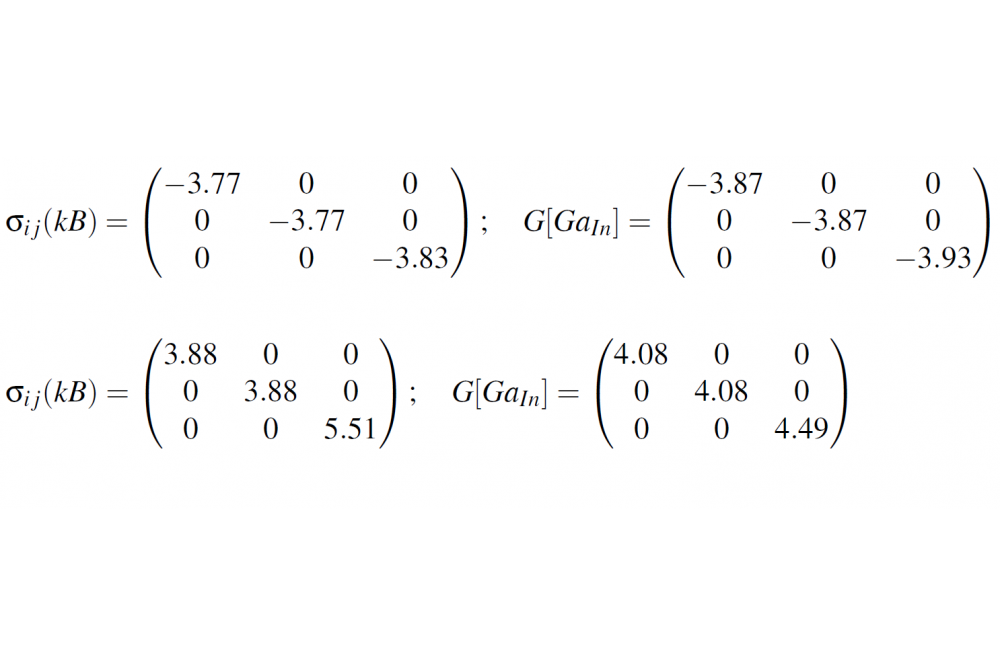
Figure 1: 1.line the components of the stress tensor σij and elastic dipole tensor of the GaIn antisite in CuInSe2 and 2. line for InGa antisite in CuGaSe2.
Elaheh Ghorbani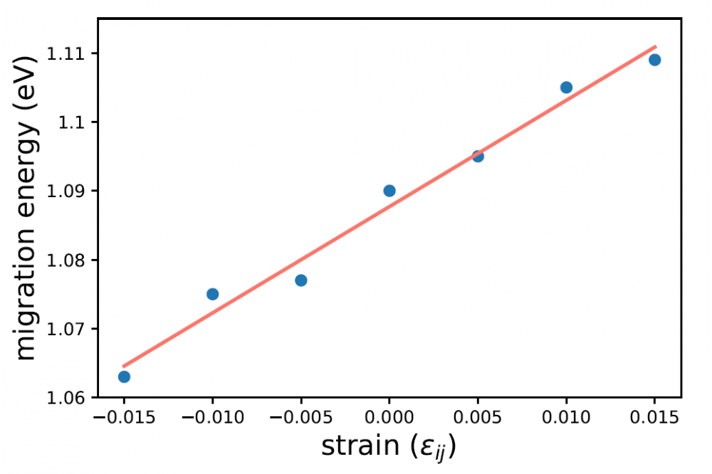 Ghorbani_Elaheh_Intermediate bands in indium thiospinels_Figure2
Figure 2: Migration barrier of In along the InCu +VCu →VCu + InCu, under various strain conditions along (110) plane. The blue circles are calculated values and the red line indicates a linear fit.
Elaheh Ghorbani Ghorbani_Elaheh_Intermediate bands in indium thiospinels_Figure3
Figure 3: Migration barrier of In and Ga in CuInSe2 and CuGaSe2 absorber materials.
Elaheh GhorbaniIntroduction
In Cu(In,Ga)(S,Se)2 (CIGS) thin-film solar cells, Ga gradient forms readily during the CIGS growth resulting to a high [Ga]/([Ga]+[In]) (GGI) ratio close to the back contact and a small GGI ratio in the middle and front sides of the absorber layer. A low Ga concentration leads to a low energy band gap. Hence, the band gap in the middle and front parts of the absorber are below the optimum value, which consequently leads to a reduced open circuit voltage at these regions. To reduce GGI variation across the film, spontaneous interdiffusion of In and Ga must be facilitated. However, since the motives for the occurrence of Ga gradient are not understood yet, finding a solution for this efficiency-limiting phenomena has not been proposed. Due to different atomic radii of In and Ga, occupying III+ cation sites by In/Ga can create different local elastic distortions. As a result, occupation of an In site by Ga (or Ga site by In), can generate a significant internal built-in strain. The present strain can cause lattice deformations and distortions and consequently have a pronounce effect on diffusion profiles of In and Ga in the CIGS. Therefore, to understand reasons behind formation of Ga gradient, a detailed knowledge of the influence of strain on mobility of In and Ga is essential.
Methods
In the present work, we discuss the diffusion of In and Ga in CuInSe2 and CuGaSe2 under strain and in the presence of Na interstitial. All calculations were carried out with plane-wave code VASP using projected-augmented wave method and PBE functional. The wave functions were expanded up to a cutoff energy of 400 eV. The activation barriers, i.e. the energy difference between the initial point of the given reaction and the transition state, were computed employing the nudged-elastic-band (NEB) in a 64-atom supercell with a k-mesh of 2×2×2. The structures were allowed to relax until the forces on each atom fell below 0.01 eV/ Å.
Results
In general, defects induce lattice distortions on both local- and long-range scales. In the specific case of point defects, the long-range elastic distortions can be completely described by means of the elastic dipole tensor (EDT). This tensor bridges the atomic structure of the defect with the elastic field it introduces in a material. Consequently, such mathematical entity also describes the interaction of point defects with strain or stress within linear elasticity. In order to understand the concept behind this tensor and how to calculate it, we analyze a truncated Taylor expansion of the energy E(nd,ɛ) of a supercell, without entropy contributions, in terms of the strain (with components ɛij) and the number of defects per supercell, nd. If the entropy contributions are neglected, the expansion of the energy density reads as:
E(nd,ɛ) = E0+½ Ʃi,j,k,l Ci,j,k,lɛijɛkl + nd (Ed –Ʃi,j Gijɛij+...
Here, E0 is the total energy of the non-strained defect-free system, Ed is the formation energy of a defect, Cijkl are the components of the stiffness tensor, and Gij is the elastic dipole tensor (EDT). Gij describes the interaction of the defect with a strain field. The positive and negative EDT components imply emergence of respectively dilation and compression centers introduced by defect. The change in energy under strain, caused by formation of a defect is then given by
ΔE = – ƩijGijɛij.
Therefore, if the elements of EDT and strain have the same (opposite) sign, the formation energy of the defect would decrease (increase). To compute the components of the EDT using the atomistic methods, we use the equation
Gijkl = – V0Δσij,
where V0 is the volume of the supercell containing one defect, and Δσij is the difference between stress of the defective and pure cells. In a periodic supercell, an isolated defect is added and the atomic positions are relaxed and the stress induced by the defect is calculated. Then, the EDT can be obtained using the Eq. 3.The components of the stress tensor σij and elastic dipole tensor of the GaIn antisite in CuInSe2 and for InGa antisite in CuGaSe2, we obtained are shown in Figure 1. As we can see, the diagonal components of the EDT of GaIn are negative. This is caused by the smaller effective ionic radius of Ga compared to that of In. Therefore, the formation energy of GaIn would decrease under a compressive strain. Reversely, for InGa, the diagonal components of EDT are positive and its formation energy would decrease under a tensile strain. A comparison between the EDT of GaIn and InGa shows that under the same amount of strain but with an opposite sign, the formation energy of InGa in CuGaSe2 would decrease more rapidly than that of the GaIn in CuISe2. To gain insights on how diffusion barrier changes under strain, we studied diffusion of In via Cu vacancy (VCu) in CuInSe2 under various strain conditions along the (110) plane. Our results (as shown in Figure 3) indicate that the diffusion barrier decreases under compressive strain, however, the reduction is very small. To check influence of Na on diffusivity of In and Ga, we studied diffusion of In and Ga in CuInSe2 in the presence of Naint. Here, we considered the diffusion paths: InCu +VCu→VCu + InCu in CuInSe2 and GaCu + VCu →VCu + GaCu in CuGaSe2. In both cases, a Naint was added to the next neighbour position of the VCu. Our calculations show that during the geometry optimization and in a barrierless recombination Na goes to the Cu vacancy. This is in contrast to Colombara’s postulation that presence of Naint enhances In/Ga interdiffusion through VCu.