Ab-Initio Calculation of Fundamental Properties of Strained Heterostructures
Introduction
Many opto-electronic devices, such as laser diodes, solar cells or semiconductor sensors, comprise of semiconductor layers. For such heterostructures great flexibility is provided by choosing appropriate materials and layer structures. Hence, the number of potential realizations is too large for simple experimental trial-and-error. Thus, it is necessary to thoroughly understand the physics of these devices and analyze their properties. Multinary semiconductor layers are the materials of choice in many cases. Determining the confinement of carriers in layers and the transport across interfaces, a critical and often controversially discussed property in a heterostructure is the band offset. For heterostructures consisting of multinary semiconductor layers, for example AB_{x}C_{1-x}, which are grown highly lattice mismatched onto a substrate, the band offsets generally do not have an easily to deduce dependency on the concentration, e.g. x. As well, in contrast to unstrained natural band offsets, they are not transitive for differing strain conditions. Calculating band offsets for heterostructures with multinary layers in dependence on the concentration of certain atoms requires large supercells. This exceeds the computational power of usual computer systems or smaller super computers.
Methods
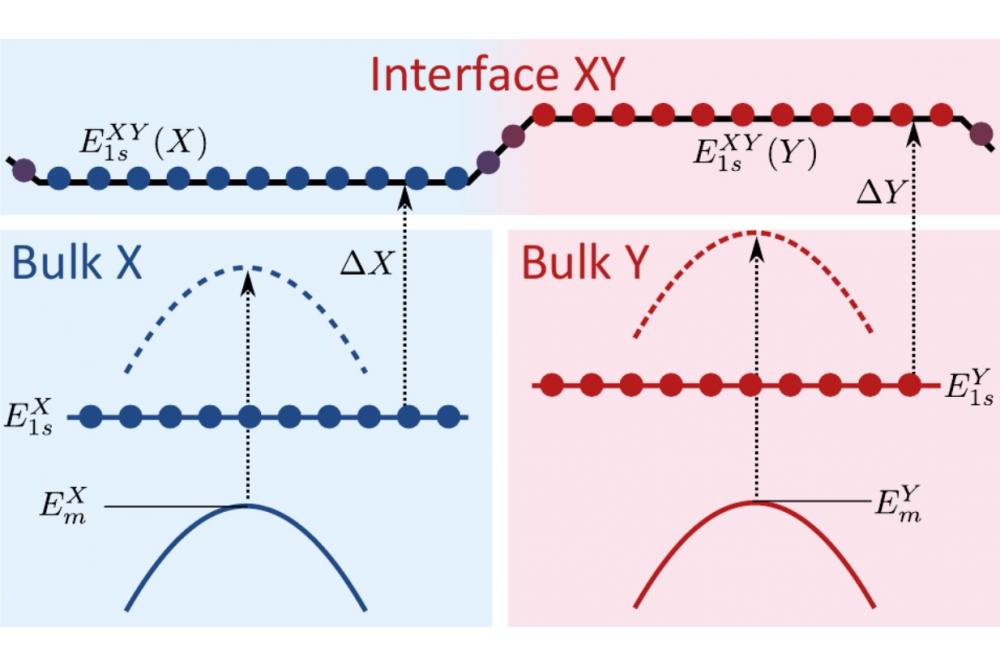
To gain insight into the band alignment of two multinary semiconductor materials we calculate the valence band offsets (VBO) of them. The VBO is the energetic difference of the valence band maxima (VBM) between the materials. For the VBO we perform bulk and interface DFT calculations. Therefore, the bulk cells of the two materials are relaxed in growth direction but strained to the substrate in the plane perpendicular to it. Subsequently, the VBMs are calculated in electronic structure calculations. Since the energy scales of the separate bulk DFT calculations are misaligned by an unknown factor, we can not simply subtract the VBMs. A common energy reference level in both systems is required to align their energy scales. We use the energy level of the core 1s electrons since they are sufficiently localized and insensitive to more distant structural features, such as hetero interfaces. Thus, the relaxed bulk cells are stack onto each other and relaxed in growth direction. This takes into account corrections of the atomic structure at the interface. Subsequently, the core levels are gained from an electronic structure calculation. The images of the core 1s levels from bulk and interface calculations are compared sufficiently far away from the interface. We use the differences in each material to align their energy scales, which enables us to determine the VBO.
Results
We tested the the method on the well-known GaAs/(Al,Ga)As interface and validated its applicability. We applied the method for the calculation of the VBOs in (In,Ga)As/GaAs/Ga(As,Sb) multi quantum well structures, which are currently examined for type II semiconductor lasers. The calculated VBOs are confirmed by comparing the experimental photoluminescence (PL) of such a structure with the calculated PL using our results.
Discussion
The results confirm the suitability of the method for the calculation of strained VBOs. The use of the calculated band offsets in connection with theoretical calculation of optical properties enables to calculate optical properties of heterostructures without experimental input.
Outlook
The results for GaAs/Ga(As,Sb) around 25% Sb suggest a dependency on the atomic arrangement. This is currently under investigation. A comparison of VBO dependency of GaAs/Ga(Bi,As) to GaAs/Ga(As,Sb) is under investigation.


